


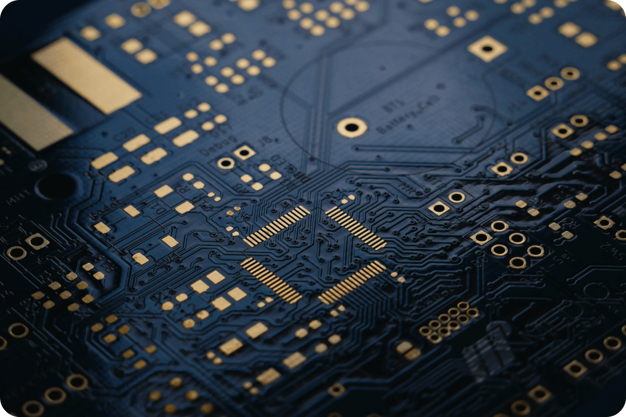
Sending your PCB design to the manufacturer is an exciting moment. After all the hard work you've put into designing and prototyping your board, it's finally time to see it come to life. But before you hit the “send” button, there are a few things you need to check first.
1. Check the board dimensions and tolerances.
Ensure it will fit into the intended enclosure, as well as any connectors or other components it will need to mate with. The last thing you want is for your board to be too big or too small for its intended purpose.
Cutout areas have to be properly defined, and otherwise you will get the board carved just along the outer edges. If the panelization is done by your manufacturer, ensure that they will install the perforated tabs in the correct locations so that any remains will not interfere with your device's housing. And don't forget to check the tolerances your manufacturer claims, which might differ significantly.
2. Ensure that your power and ground planes are properly connected.
When it comes to ensuring power integrity in your circuit boards, there are a few key things you need to keep in mind. First, you have to make sure that all power and ground nets are connected to proper planes and polygons. This will help to ensure that currents can flow freely and that sensitive circuits are protected from interference.
Additionally, you must have sufficient decoupling capacitors in your design. These capacitors are helping to isolate sensitive circuits and prevent them from experiencing power interruptions.
3. Verify the integrity of critical signals.
Check for crosstalk, impedance mismatches, and other potential signal integrity issues. These can all cause problems down the line, so it's best to catch them early. Sensitive analog signals, in particular, need to be isolated from any potential electrical noise sources, such as switching power supplies or high-speed digital circuits.
By taking the time to check for potential signal integrity issues, you can rest assured that your device will function as intended, measurements are correct, and the wireless connection is reliable and robust.
4. Check for clearance issues.

It's important to ensure that there is sufficient clearance between all of the traces on your board. If traces are too close together, they run the risk of shorting out, which can cause all sorts of problems.
Additionally, you need to make sure that there is sufficient clearance around any exposed copper, such as vias and pads, to prevent any accidental shorts from occurring during assembly or use. This is especially important if your board handles high voltages or will be subject to high levels of heat or stress.
5. Make sure all the component footprints are correct.
Before sending your design to the manufacturer, you need to make sure that all the footprints are correct. There are a few different ways to verify footprints, but the most common is to use a tool called a “footprint manager” in your CAD.
This tool allows you to view your footprints in 2D, making it easy to spot any errors. Double-check all the drill sizes, shapes, and plating for through-hole components as well as SMD parts with mechanical pins.
6. Check for any routing errors.
Nobody dreams about their PCB being rejected because of a short or open circuit, or even worse being made with these hard-to-diagnose defects built-in. To avoid this, you need to make sure that all the nets in your design are properly connected.
You can verify this using a design rule checker in your CAD software. This tool allows you to verify the connection of all the nets in your design, making it easy to spot any errors. However, it's also useful to run DRC tests against as many rules as your CAD supports, to be on the safe side.
7. Make sure all the vias are placed correctly.
Vias are important elements in your PCB design, and you need to make sure that they're placed correctly. Ensure that all the vias are connected to the correct nets, and that they're placed in the correct locations. Vias that are placed too close to each other can cause shorts, and vias that are placed in the wrong location can cause manufacturing defects.
Another mistake that is sometimes made is forgetting to move the vias when moving the polygons. If your design requires via stitching, double-check that it has been completed.
8. Check the solder mask and silkscreen layers for errors.
The solder mask and silkscreen are important layers in your PCB design, and you need to make sure that they're free of errors. The solder mask is a layer of usually green ink that protects the copper traces from being soldered to the wrong pad. The silkscreen is a layer of white ink that is used to print labels and other information on the PCB.
Make certain that there are no errors in either of these layers, as they can lead to problems during manufacturing. If the silkscreen contains a revision number, don't forget to update it.
9. Not to overlook the specifics of flexible and semi-flexible PCBs.
If your design is for a flexible or semi-flexible PCB, there are a few things you need to keep in mind. First, the minimum trace width and spacing should be increased to accommodate the flexibility of the substrate, and curved traces are preferable. Second, the vias have to be larger to prevent cracking during bending.
Finally, the SMT pads and non-plated through-holes often require additional support tabs or anchors to prevent detachment. The finest option is to use the recommendations of the manufacturer that you've chosen for optimum performance and dependability.
10. Inspect the Gerber and NC drill files.
Before sending your PCB design off to the manufacturer, it's always a good idea to do a final check of the Gerber and drill files. This is because there is a number of potential problems that can occur during the transfer from design to production.
For example, incorrect solder mask openings can lead to shorts or bridging, while unwanted vias in SMD pads can cause reliability issues. Additionally, wrong trace widths for controlled impedance can result in poor electrical performance. Finally, overlapping drills can cause physical damage to the board during drilling. While there are automated tools available for checking manufacturing files, nothing beats a careful visual inspection by an experienced engineer.
11. Check the bill of materials for accuracy.

There are a few things to look for when verifying your BOM. First, make sure that all the component values are correct. Second, check that any components that do not need to be populated are clearly labeled as such.
This is doubly important if you are working with a contract manufacturer, as they may not be familiar with your design. It is often helpful to move these absent components to the bottom of the table with bold notice like “do not populate” or “do not install”.
Finally, if your CAD software allows it, defining multiple variants of the BOM can be a useful way to avoid errors associated with manual BOM editing.
12. Make sure you have included all the necessary files.
The files you need to include will depend on the manufacturer you're using, but there are a few that are always required. These include the Gerber files for the PCB layout, the NC drill files, and the bill of materials.
You'll also have to supply a pick and place and any design files required for the assembly process. If you're using a contract manufacturer, they will usually have a list of the needed files. They also provide an order form where layer stackup, PCB materials, and plating are specified.
13. Have someone else review your design to catch any errors you may have missed.

Even if you've followed all the steps above, it's always a good idea to have someone else review your design. This is because it's easy to overlook errors when you're familiar with the design.
A fresh set of eyes can often catch things that you've missed. If possible, it's best to have the design reviewed by someone with experience in PCB design and manufacturing.
14. Make sure you are happy with your design before sending it off to be manufactured!
You've put a lot of time and effort into your design, so it's important to make sure you're happy with it before sending it off to be manufactured.
If you have concerns, it's usually a good idea to make modifications to the design before submitting it to the manufacturer. This will help to ensure that you're happy with the final product.
Conclusion – It's All About Saving Your Money and Releasing the Product Faster.
Making a PCB is not an easy task, and it requires a lot of knowledge, expertise, and experience. If you want to ensure your product's success, you need to invest the time in checking your design and making sure it is ready for manufacturing.
This will save you from doing unnecessary debugging and rework down the road. If you are unsure about how to do this or would like professional help, feel free to reach out to us. We at Embedity would be happy to assist you with your PCB design needs.
.jpg)


